


Address:RM1507,15rd Floor,Bldg B,TANGSHANG building,No.35 guangshen Rd,Bao
Current position:Home >ODM > Envelope Foundry >
Types of package introduction
Ⅰ.DIP(Dual-in-line Package)
SDIP :Shrink dual in-line package, pin density is higher than common DIP
PDIP :Plastics dual inline package, the distance between two pins is small than common ones, known as slim DIP
Ⅱ.QFP (Quad Flat Package)
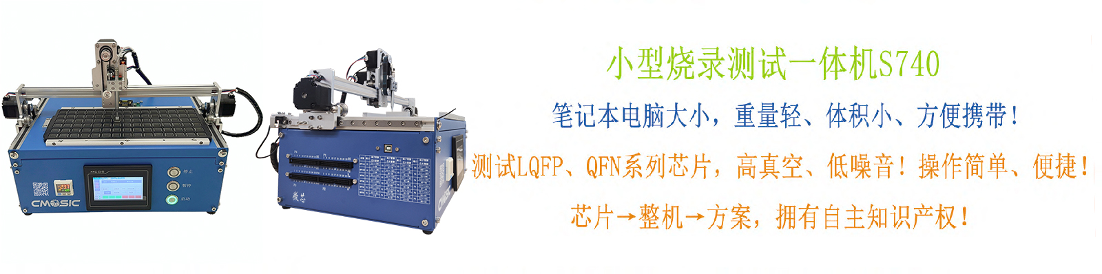
LQFP :Little QFP,simplify number of pins,apply for limited space
TQFP :Thin QFP, shrink height
CQFP :Ceramic QFP, pins spread out from inner to all direction parallel
VQFP :Very thin QFP
HQFP :Heat sink QFP
PQFP :Plastic QFP
Ⅲ.SOP (Small Outline Package)
SOP (Small Outline Package)
Ⅳ.SOJ (Small Outline J-lead)
Ⅴ.LCC (Leaded Chip Carrier)
PLCC :Plastic LCC
Ⅵ.BGA (Ball Grid Array package)
PBGA :Plastic BGA
CBGA :Ceramic BGA,chip and substrate usually adopt Flip Chip installation
FCBGA :Flip Chip BGA,hard multi-layers of organic material
TBGA :Tape BGA,tape soft material
CDPBGA :Carrier Down PBGA, cavity in central package
Ⅶ.PGA (Pin Grid Array package)
Ⅷ.CSP (Chip Scale Package)
Ⅶ.SOT (Small Outline Transistor package)
 86-19575121554